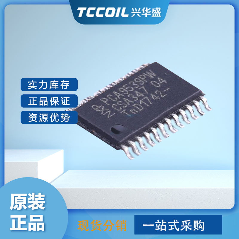
接口 - 控制器
型号:SJA1000T/N1
封装:SOP28

FUNCTIONAL DESCRIPTION System clock The UDA1361TS accommodates master and slave modes. The system devICes must provide the system clock regardless of master or slave mode. In the master mode a system clock frequency of 256fs is required. In the slave mode a system frequency of 256, 384, 512 or 768fs is automatically detected (for a system clock of 768fs the sampling frequency must be limited to 55 kHz). The system clock must be locked in frequency to the digital interface input signals. Input level The overall system gain is proportional to VDDA, or more accurately the potential difference between the reference voltages VVRP and VVRN. The ?1 dB input level at which THD + N/S is specified corresponds to ?1 dB(FS) digital output (relative to the full-scale swing). With an input gain switch, the input level can be calculated as follows: at 0 dB gain: at 6 dB gain: In applications where a 2 V (RMS) input signal is used, a 12 kΩ resistor must be connected in series with the input of the ADC. This forms a voltage divider together with the internal ADC resistor and ensures that only 1 V (RMS) maximum is input to the IC. Using this application for a 2 V (RMS) input signal, the gain switch must be set to 0 dB. When a 1 V (RMS) input signal is input to the ADC in the same application the gain switch must be set to 6 dB. An overview of the maximum input voltage allowed against the presence of an external resistor and the setting of the gain switch is given in Table 1. The power supply voltage is assumed to be 3 V
